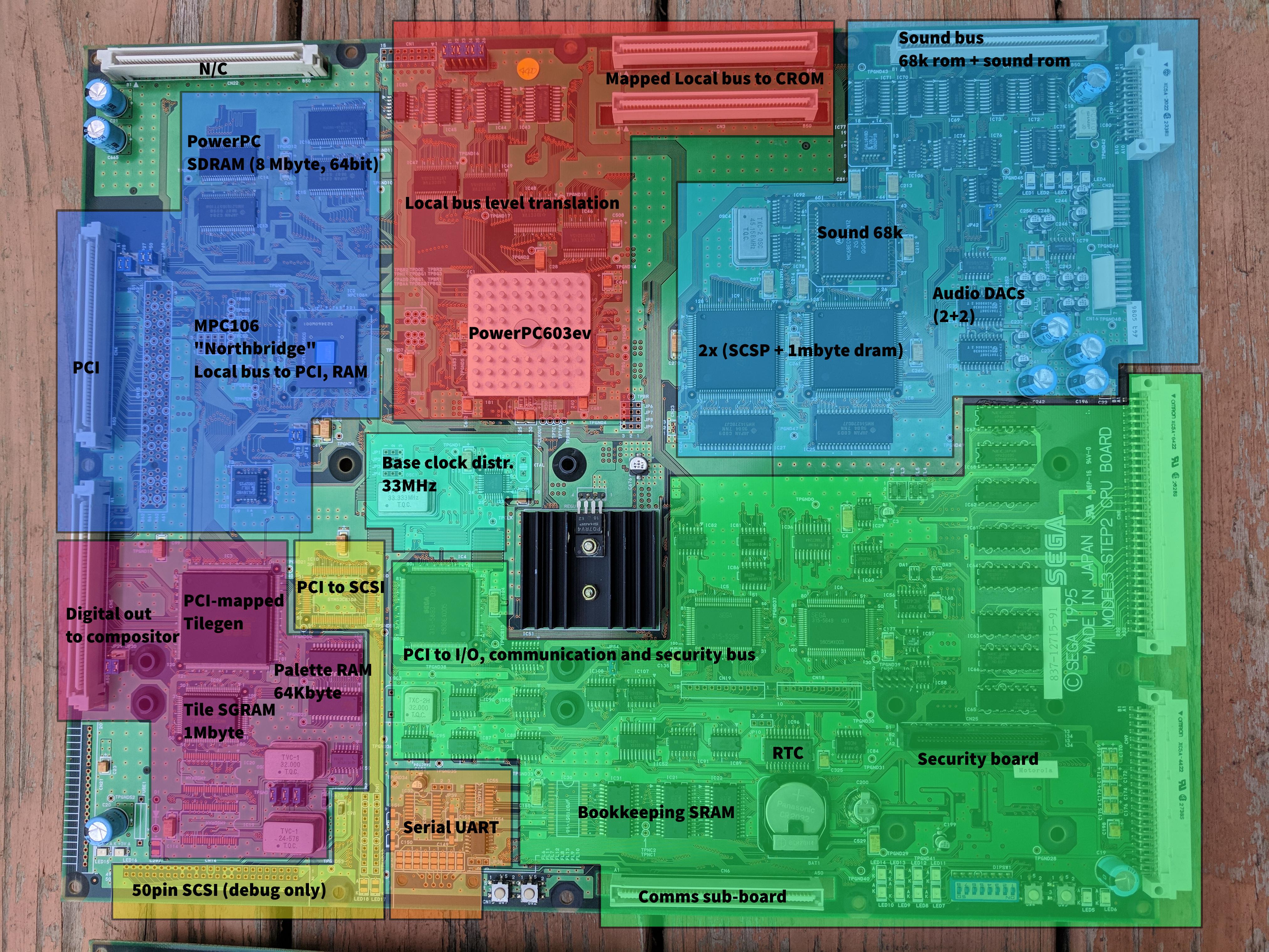
The PCI footprint is probably a leftover from early DVT and, like the service buttons and various jumpers, were never removed as each board was expensive enough to justify a tech touching it for go/nogo production.
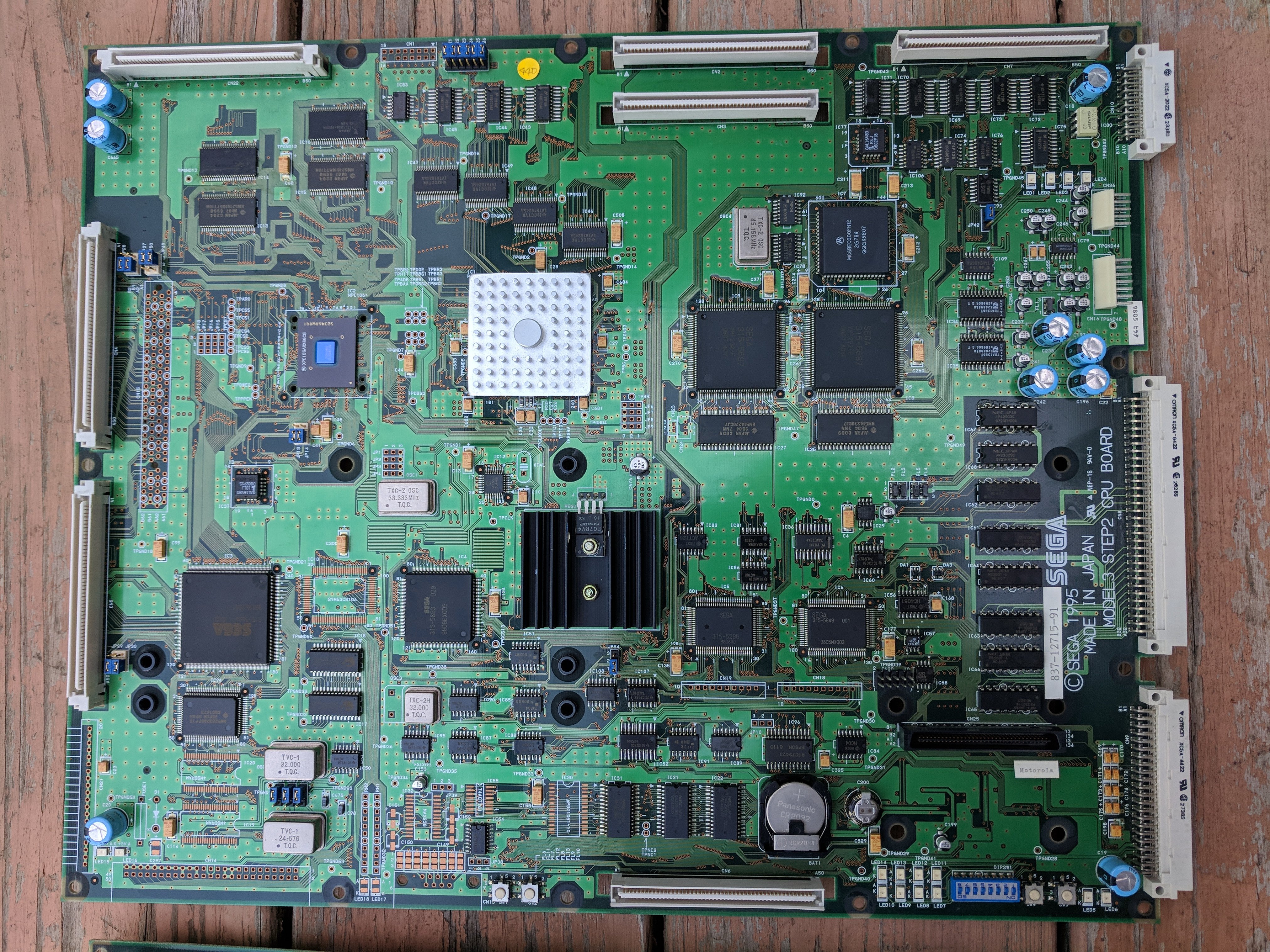
CPU Board
The 2x SCSP configuration was also used on Cool Riders (System H1) and also 1x SCSP used on the rare Flash Beats rhythm game.
Security board on the HD68 connector is a 315-5881 microprocessor with some sram and GALs. The 315-5881 was integrated into Hikaru games as well as Naomi carts. The same connector is also present but unused on System H1 (Cool Riders). It seems to be reflashable. PowerPC can dma data to/from this processor to decrypt it before uploading it to the 2d tilegen (Dirt Devils, others)
Present, but unpopulated:
Symbios SYM53C810A PCI-SCSI bridge. Step1 seems to have leftover bits of SCSI stuff in the ppc code, was it actually used for anything, or just a remnant of dev? It's present on Step1, but its connector still is missing.
MAX232 serial UART and DB9 connector. PPC code is full of debug printfs as usual. Would be fun to see those going during gameplay.
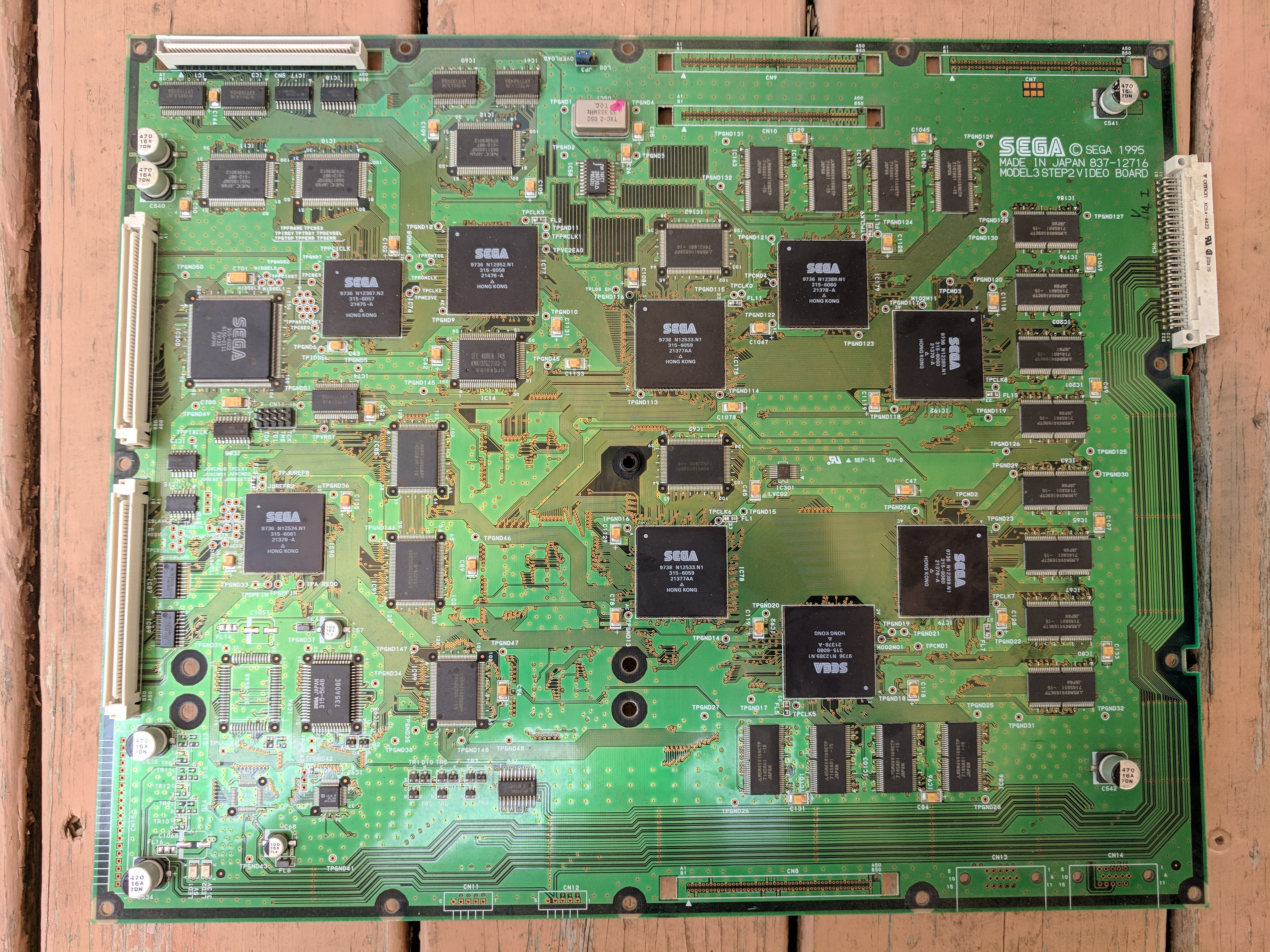
Fullsize https://i.imgur.com/clU3y8q.jpg

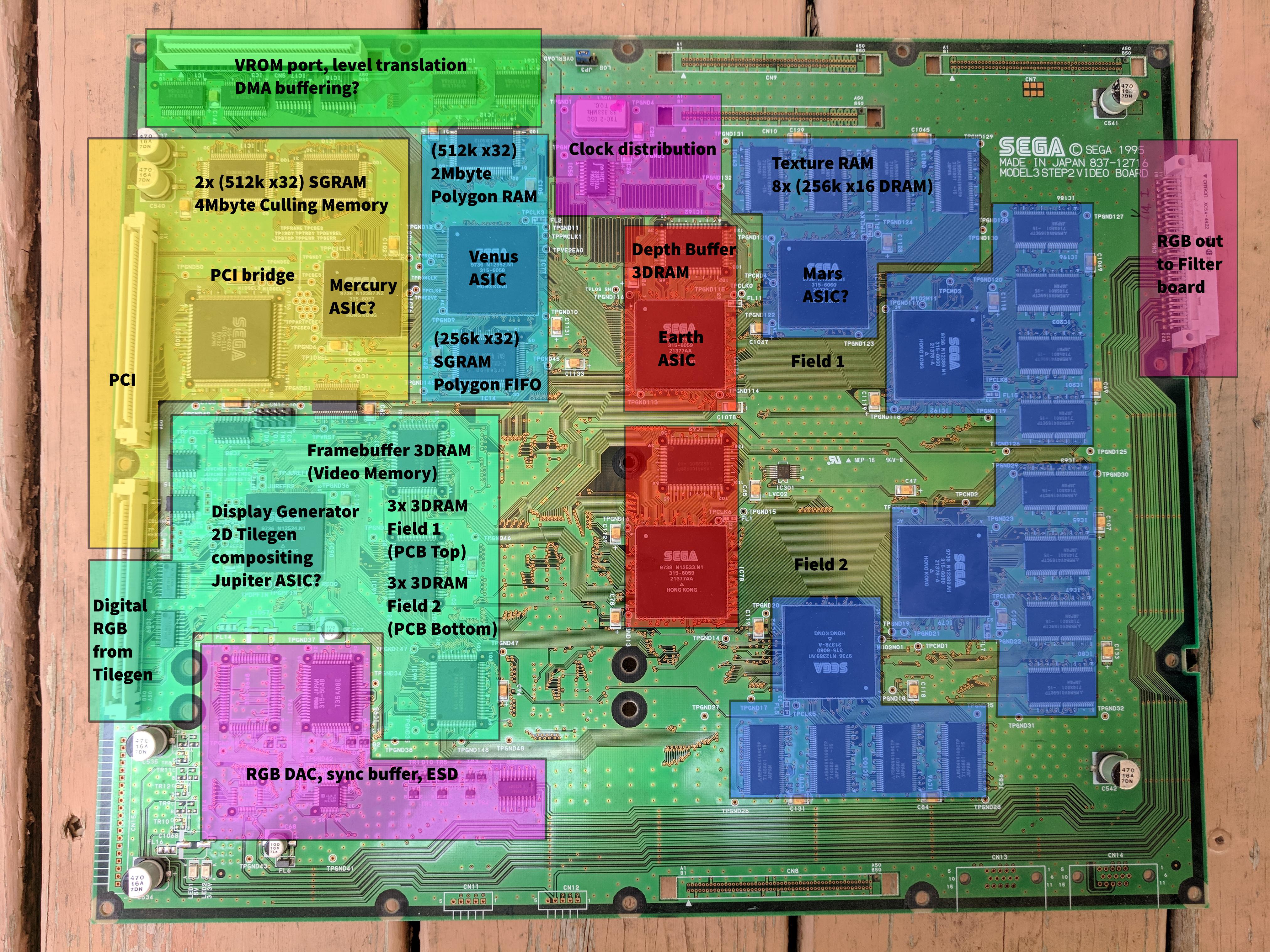
Real3D board
By opening the Real3D Pro/1000 firmware image from the Lockheed sdk and analyzing it, I saw codenames for a lot of the asics in debug prints. Funny enough - they are all planet names of the solar system, starting from the inside of the system (Mercury) and working outwards in the solar system as the graphics data is produced along the pipeline.
Then, I booted my Daytona2 boardstack with various pins shorted on each ram to determine which rams where labeled as what, in the memory test. Further combined with my spotty knowledge about 90s fixed function GPU architectures, here are my thoughts on theory of operation:
Starting at the beginning of the pipeline --
PCI bridge - probably a NEC/Fujitsu gate array. Sega-designed, since it is not fabbed in Hong Kong like the rest of the Real3d chipset.
Mercury & Venus - I am a bit unclear on the role of this and Venus. But we know that most scenegraph data will be stored in VROM statically and accessed on demand - in fact, the VROM bus is synchronous and accessed faster than the asynchronous CROM or SROM. Additionally, some games upload dynamic mesh data on a per-frame basis. The culling processor is to take the camera position in the scenegraph and emit polygons contained in the view frustrum and nothing but, so dynamic mesh data probably lives in one of those SGRAMs. Mercury probably stores dynamic scenegraph data like transformation matrices for all the models and attribute data that changes at runtime. However, it may be possible that mesh data is not streamed and instead must live entirely in culling RAM - this is what Real3D does, and it has 8Mbyte. Mercury probably does scene graph traversal and rough rejection, Venus probably runs a DSP (is firmware loaded over jtag? or is it mask only) doing vertex T&L and passing 2d triangles to Earth.
From here the polygons are split into two identical rasterization pipelines, which are set up in scanline interleave ala nvidia SLI. Each set handles one field (odd or even scanlines)
Earth - rasterizer (edge/span walker and depth rejection). The service menu list the Mitsubishi 3dram connected as the depth buffer, so Zbuffer compares happen here. Additionally, each Earth chip is connected to its own set of 3x mitsubishi 3drams which are used as the framebuffer, probably split into R/G/B components. Interestingly, the rams have integrated pixel ALUs to support blending over existing framebuffer data. This prevents the Earth chip from ever having to readback the existing framebuffer data for a RMW blending cycle. Doing it this way makes Z-buffering incur no performance penalty and means draw order doesn't matter (No early z-sort necessary). Of course, this makes the rams a lot more complex, and worth a look in themselves...
Mars - texturing unit. Each ASIC is wired to 4 megabytes of DRAM, for an effective bus width of 128 bits. Each Earth chip has two of these texturing units. However, there are a number of ways they could have set up their texturing - Real3D overview says low-end units had 8MB of texture memory. So my guess is that there are only 4Mbytes of unique texture memory, and it is duped multiple times over each of the 4x Mars chips. This is to perform multiple lookups per cycle, which is a key part of mipmapping. The Real3D docs state that the system does support trilinear filtering with mipmapping, so you do need to LERP between two set of texture samples per cycle - the larger mipmap and the smaller one. The parent Earth chip interpolate the two texels and sends the shaded fragment to the framebuffer where it is blended with existing framebuffer contents.
The line size is 128 bits - which at 16bpp works out to 8 pixels. However, these DRAMs are actually special Mitsubishi "Cache DRAMs", which basically incorporates a 1K texel cache. So instead of putting cache on the ASIC they likely use this one in the memory. You can load the cache and then start another fetch while reading it out. The cache would provide a 32x32 block, which when doing the right texture swizzling is a pretty respectable amount (This is also the minimum supported texture size by Real3d). However, the texture layout in RAM could be done many different ways that would all be transparent to software.
Here is where the Sega implementation starts to differ considerably from the Lockheed one - Real3D has a "scroll layer" that shows 2d elements like sky backgrounds. This is part of the Jupiter chip. However, Sega decided to swap in their System24 2d PPU which was also used in the previous Model 2. This lives on the CPU board and is completely separate, but the frame timing lined up so it emits pixels at the same rate.
Jupiter - Sega's modified Jupiter doesn't have any 2d generation in it, but it reads out the 3d framebuffer and composites this with the 2d PPU output, which is digital RGB. The composited output is sent to the video output DAC turning into standard analog rgb. Both 3d odd/even video fields are interleaved into progressive output. I am not sure what the Sega 315-5648 chip is doing - maybe it's for deinterleaving stereo crts? There is space for another DAC for dual outputs. This chip was also used on Model2 and System H1 boards.
Fullsize https://i.imgur.com/n42LCxO.jpg

https://www.bloomberg.com/press-release ... hics-chips
Clock rates for Real3d seem to be 50MHz on Pro/1000 as well as Step 1.0. Step 1.5 seems to be 66MHz. My Step 2.0 boards have a 33mhz oscillator so they may be 66MHz as well. So just doing some guessing, that puts the fill rate of this system at 133 Mpixel/sec. If the clock rate was increased too 100mhz, two pipelines means 200Mpix/sec fillrate.
A very interesting board, and the discrete architecture is neat in the current age of wholly-integrated SoCs and other such boring stuff.
