Shift-DR, Exit1-DR, etc. are just states in the state machine. JTAG allows for arbitrary length data and instruction registers that are loaded up one bit at a time via a serial protocol that involves a clock to shift one bit at a time and then a signal called TMS which is used to transition to the next state. Shift-DR shifts into (and out of) whatever data register is selected by the current contents of the instruction register. My logging might be buggy. I'm incrementing a bit counter on each Shift-DR tick and each time it gets to 32, I print out the last 32 bits and reset. I also then do it again on Exit1-DR, which is an intermediate state when shifting is done, to log any remaining bits. I might need to rewrite the JTAG code from scratch to be a little clearer and more flexible. It's now only designed to shift out the ASIC ID codes.
The state machine is conceptually simple. The software makes two writes in order to drive the machine once: first, it writes data with the CLK bit 0 and then it writes it again with 1. The transition from 0->1 is what advances the machine (because underneath, that CLK bit is tied to an actual CLK signal in the digital logic that comprises the TAP port). In addition to the clock, there is a TDI bit which is the data being supplied as input (for those states that use it) and a TMS bit which determines where the state machine will go on the next clock cycle. Each state can advance to one of two next states based on TMS being 0 or 1. Often times, one of those two states is the current state (as in Shift-DR and Shift-IR).
The complexity lies in the fact that we have no idea how many data registers there are, what their sizes are, etc. The protocol doesn't define any of that. Theoretically should be possible to deduce with proper logging by seeing how many bits are shifted for a given instruction. But I think I've seen some weird behavior that doesn't make complete sense to me.
Here's the state machine:
And here's the state machine with a schematic block diagram of what an actual implementation circuit would look like:
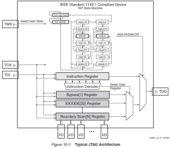
Not sure how familiar you are with digital logic but this is really simple if you look carefully. The TDI bit is fed into all these shift registers simultaneously (instruction register and all data registers that the designers decide to create). As you clock the state machine in the shift IR or shift DR state, all the registers get loaded up simultaneously.
IR (instruction register) is fed into a decoder which looks at the value and produces a signal into the multiplexer that all data registers feed into. Only one of those data registers is selected and allowed to pass through. Lastly, even that is multiplexed with the instruction register based on whether you were in Shift-DR or Shift-IR to shift back out via a TDO bit to the CPU for when it wants to read. I think there is one thing missing here and that is the Capture/Update states. This diagram suggests the boundary scan registers, which would connect directly to device IO pins, are always connected, which cannot be correct. I think there is a state that happens after you finish shifting in the data register which then actually allows that register to output its values to whatever it's connected to.
With this simple scheme, the designers of an ASIC can implement any kind of debug functionality they want, including access to internal chip signals for hardware engineers to perform live testing on.